SCHMITT-NOT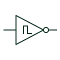
Schmitt-trigger inverter
A digital inverter with hysteresis between its input switching thresholds.
Schematic
IEC inverter with the hysteresis mark, used to clean up slow edges while inverting the signal.
In plain English
This element combines the 1 additional drawing mark, the hysteresis mark and output negation. It inverts the signal while switching at two thresholds, which makes it a common choice for debouncing contacts with an RC network and for building simple relaxation oscillators.
When a Schmitt inverter forms part of an oscillator or delay with external resistors and capacitors, the drawing should keep those components next to the element and note the intended timing. The symbol alone gives no clue that it is part of a timing circuit.
Thresholds, hysteresis width and supply range are device data. Different logic families have markedly different thresholds even though the symbol is identical.
IEC inverter with the hysteresis mark, used to clean up slow edges while inverting the signal. The Schmitt buffer has the same hysteresis mark but no output negation.
Read the source: Overview of IEEE Standard 91-1984: explanation of logic symbols (SDYZ001A) · SN74HC14 — Schmitt-trigger inverters
Qualifying-symbol and dependency conventions as explained in TI's public overview of IEEE Std 91-1984, which incorporates IEC 617-12 work. Independent educational drawing; not certified IEC geometry or an IEC database identifier. The counterpart is the matching functional concept; no equivalence of every detailed standard graphic is asserted.
Shown as an independently authored educational illustration. Use the cited publication and drawing legend to verify the required drafting form.
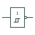
This element combines the 1 qualifier, the hysteresis mark and output negation. It inverts the signal while switching at two thresholds, which makes it a common choice for debouncing contacts with an RC network and for building simple relaxation oscillators.
When a Schmitt inverter forms part of an oscillator or delay with external resistors and capacitors, the drawing should keep those components next to the element and note the intended timing. The symbol alone gives no clue that it is part of a timing circuit.
Thresholds, hysteresis width and supply range are device data. Different logic families have markedly different thresholds even though the symbol is identical.
The Schmitt buffer has the same hysteresis mark but no output negation.
These public references support the explanation and provide further detail. Their graphics and downloadable files remain with their publishers.
Hysteresis and negation qualifiers.
Manufacturer Schmitt-trigger inverter documentation.
This illustration was authored independently by Elora Grid to explain the concept. It is not reproduced from a customer drawing, an official standard graphic or a manufacturer CAD file. Its correspondence to an exact IEC or IEEE symbol identifier has not been certified.
SVG and DXF downloads contain this original artwork. DXF uses unscaled drawing units; a GA envelope supplies no product dimensions, clearances or fabrication information. Original artwork is available under CC BY 4.0. Third-party references retain their own terms.
A digital inverter with hysteresis between its input switching thresholds.
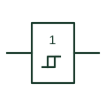
Rectangular buffer carrying the hysteresis mark, meaning its input switches at two different thresholds.
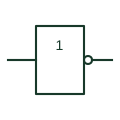
Single-input IEC box marked 1 with a negation at the output, inverting the logic state.
Elora Grid helps electrical teams work with drawings, specifications and equipment information. Explore the drafting workflow or join the early-access waitlist.