D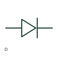
Diode
A diode provides a semiconductor path with documented directional conduction characteristics.
Schematic
Tunnel diode form: Tunnel Diode.
In plain English
A tunnel diode has a heavily doped junction whose current-voltage characteristic includes a negative differential-resistance region caused by tunnelling. This entry identifies the tunnel diode form in the publisher's IEC-context family.
An oscillator or fast switching circuit can bias the junction in the required region. The bias network is essential to understanding why this device behaves differently from a normal rectifier.
A tunnel diode is distinct from a Zener diode: the useful characteristic is its negative-resistance region rather than a specified reverse breakdown clamp.
Tunnel diode form: Tunnel Diode. This entry adds the tunnel diode detail to the broader tunnel diode family. A tunnel diode is distinct from a Zener diode: the useful characteristic is its negative-resistance region rather than a specified reverse breakdown clamp.
Read the source: AutoCAD Electrical: Semiconductor components
Autodesk IEC-60617 Symbol Preview: Semiconductor Components, HDI1_S00645 / VDI1_S00645. This identifies the publisher's library context; exact IEC graphics and database identities are not asserted.
Shown as an independently authored educational illustration. Use the cited publication and drawing legend to verify the required drafting form.
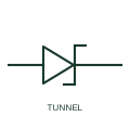
A tunnel diode has a heavily doped junction whose current-voltage characteristic includes a negative differential-resistance region caused by tunnelling. This entry identifies the tunnel diode form in the publisher's IEC-context family.
An oscillator or fast switching circuit can bias the junction in the required region. The bias network is essential to understanding why this device behaves differently from a normal rectifier.
A tunnel diode is distinct from a Zener diode: the useful characteristic is its negative-resistance region rather than a specified reverse breakdown clamp.
This entry adds the tunnel diode detail to the broader tunnel diode family. A tunnel diode is distinct from a Zener diode: the useful characteristic is its negative-resistance region rather than a specified reverse breakdown clamp.
These public references support the explanation and provide further detail. Their graphics and downloadable files remain with their publishers.
Public Semiconductor Components table explicitly lists HDI1_S00645 / VDI1_S00645 with this operating or connection form. Vendor graphics are linked, not copied.
This illustration was authored independently by Elora Grid to explain the concept. It is not reproduced from a customer drawing, an official standard graphic or a manufacturer CAD file. Its correspondence to an exact IEC or IEEE symbol identifier has not been certified.
SVG and DXF downloads contain this original artwork. DXF uses unscaled drawing units; a GA envelope supplies no product dimensions, clearances or fabrication information. Original artwork is available under CC BY 4.0. Third-party references retain their own terms.
A diode provides a semiconductor path with documented directional conduction characteristics.
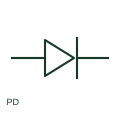
A photodiode is a light-sensitive semiconductor device used in a documented sensing circuit.
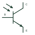
An NPN transistor whose collector-emitter conduction responds to incident light in the documented detector arrangement.
Elora Grid helps electrical teams work with drawings, specifications and equipment information. Explore the drafting workflow or join the early-access waitlist.