NAND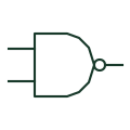
NAND gate
A logic gate that inverts the result of an AND operation.
Schematic
NAND outline with a hysteresis mark inside, combining the NAND function with Schmitt-trigger inputs.
In plain English
A Schmitt-trigger NAND is drawn as a normal NAND outline with the hysteresis mark inside the body. Each input switches at different rising and falling thresholds, so the gate accepts slow or noisy signals while still performing the NAND function.
These gates are often used for gated oscillators, where one input enables an RC oscillator built around the gate, and for combining a debounced contact with an enable signal. Timing components should be drawn close to the gate with the intended frequency or delay noted.
Threshold levels and hysteresis width are not shown by the symbol and differ between logic families. Read them from the device documentation.
NAND outline with a hysteresis mark inside, combining the NAND function with Schmitt-trigger inputs. A standard NAND has no hysteresis mark and a single threshold.
Read the source: SNx4HC132 quadruple 2-input NAND gates with Schmitt-trigger inputs
Distinctive-shape form as used in IEEE/ANSI-style schematics and manufacturer data books. Independent educational drawing; exact standard geometry and compliance are not asserted.
Shown as an independently authored educational illustration. Use the cited publication and drawing legend to verify the required drafting form.
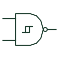
A Schmitt-trigger NAND is drawn as a normal NAND outline with the hysteresis mark inside the body. Each input switches at different rising and falling thresholds, so the gate accepts slow or noisy signals while still performing the NAND function.
These gates are often used for gated oscillators, where one input enables an RC oscillator built around the gate, and for combining a debounced contact with an enable signal. Timing components should be drawn close to the gate with the intended frequency or delay noted.
Threshold levels and hysteresis width are not shown by the symbol and differ between logic families. Read them from the device documentation.
A standard NAND has no hysteresis mark and a single threshold.
These public references support the explanation and provide further detail. Their graphics and downloadable files remain with their publishers.
Manufacturer documentation for NAND gates with Schmitt-trigger inputs.
This illustration was authored independently by Elora Grid to explain the concept. It is not reproduced from a customer drawing, an official standard graphic or a manufacturer CAD file. Its correspondence to an exact IEC or IEEE symbol identifier has not been certified.
SVG and DXF downloads contain this original artwork. DXF uses unscaled drawing units; a GA envelope supplies no product dimensions, clearances or fabrication information. Original artwork is available under CC BY 4.0. Third-party references retain their own terms.
A logic gate that inverts the result of an AND operation.
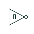
A digital inverter with hysteresis between its input switching thresholds.
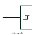
Small hysteresis loop mark showing a Schmitt-trigger function or a bi-threshold input.
Elora Grid helps electrical teams work with drawings, specifications and equipment information. Explore the drafting workflow or join the early-access waitlist.