OC-BUF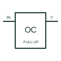
Open-collector buffer
Provides a logic output through a transistor pull-down stage requiring the documented external load or pull-up.
Schematic
Inverter triangle with output bubble and an open-circuit mark, needing an external pull-up to produce a high level.
In plain English
This is an inverter whose output transistor can only pull low. On distinctive-shape schematics the triangle and bubble are retained and an open-collector or open-drain mark, often the underlined diamond, is placed inside or beside the outline. A pull-up resistor or load to a supply completes the circuit.
Open-drain inverters are used to drive indicator LEDs, relay inputs and shared interrupt or alarm lines, and to translate to a higher pull-up voltage within the device rating. The schematic should show the pull-up value and its supply rail next to the gate.
The output state with no pull-up is undefined when the transistor is off. A drawing that omits the pull-up is incomplete even though the gate symbol is correct.
Inverter triangle with output bubble and an open-circuit mark, needing an external pull-up to produce a high level. The non-inverting open-collector buffer has no output bubble.
Read the source: SNx4HC05 hex inverters with open-drain outputs · Overview of IEEE Standard 91-1984: explanation of logic symbols (SDYZ001A)
Distinctive-shape form as used in IEEE/ANSI-style schematics and manufacturer data books. Independent educational drawing; exact standard geometry and compliance are not asserted.
Shown as an independently authored educational illustration. Use the cited publication and drawing legend to verify the required drafting form.
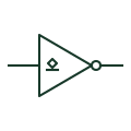
This is an inverter whose output transistor can only pull low. On distinctive-shape schematics the triangle and bubble are retained and an open-collector or open-drain mark, often the underlined diamond, is placed inside or beside the outline. A pull-up resistor or load to a supply completes the circuit.
Open-drain inverters are used to drive indicator LEDs, relay inputs and shared interrupt or alarm lines, and to translate to a higher pull-up voltage within the device rating. The schematic should show the pull-up value and its supply rail next to the gate.
The output state with no pull-up is undefined when the transistor is off. A drawing that omits the pull-up is incomplete even though the gate symbol is correct.
The non-inverting open-collector buffer has no output bubble.
These public references support the explanation and provide further detail. Their graphics and downloadable files remain with their publishers.
Manufacturer documentation for inverters with open-drain outputs.
Open-collector output qualifier.
This illustration was authored independently by Elora Grid to explain the concept. It is not reproduced from a customer drawing, an official standard graphic or a manufacturer CAD file. Its correspondence to an exact IEC or IEEE symbol identifier has not been certified.
SVG and DXF downloads contain this original artwork. DXF uses unscaled drawing units; a GA envelope supplies no product dimensions, clearances or fabrication information. Original artwork is available under CC BY 4.0. Third-party references retain their own terms.
Provides a logic output through a transistor pull-down stage requiring the documented external load or pull-up.
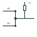
Several open-collector outputs joined on one pulled-up line, so any output pulling low makes the line low.
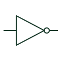
Produces the opposite logical state of its defined digital input.
Elora Grid helps electrical teams work with drawings, specifications and equipment information. Explore the drafting workflow or join the early-access waitlist.