BUF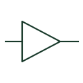
Non-inverting logic buffer
Transfers a digital state through a non-inverting logic output stage.
Schematic
Non-inverting IEC element marked 1, passing the input state to the output unchanged.
In plain English
A rectangular element with the additional drawing mark 1 and no negation simply repeats its input. It is used to show isolation between logic stages, a fan-out point, or an interface where a physical buffer device exists. When the buffer has greater than normal drive capability, an amplifier triangle pointing in the signal direction is added inside the outline.
On logic diagrams for control panels the buffer often marks where a signal leaves one card or module and enters another. Tagging the buffer with the module reference helps fault finding because it identifies the boundary at which the signal can be measured.
A plain 1 element says nothing about output type or enable. Three-state, open-collector and Schmitt variants each require an additional additional drawing mark.
Non-inverting IEC element marked 1, passing the input state to the output unchanged. The same box with output negation is an inverter; the amplifier triangle inside marks increased drive capability.
Read the source: Overview of IEEE Standard 91-1984: explanation of logic symbols (SDYZ001A) · SN74LS07 — open-collector output buffers
Qualifying-symbol and dependency conventions as explained in TI's public overview of IEEE Std 91-1984, which incorporates IEC 617-12 work. Independent educational drawing; not certified IEC geometry or an IEC database identifier. The counterpart is the matching functional concept; no equivalence of every detailed standard graphic is asserted.
Shown as an independently authored educational illustration. Use the cited publication and drawing legend to verify the required drafting form.
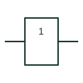
A rectangular element with the qualifier 1 and no negation simply repeats its input. It is used to show isolation between logic stages, a fan-out point, or an interface where a physical buffer device exists. When the buffer has greater than normal drive capability, an amplifier triangle pointing in the signal direction is added inside the outline.
On logic diagrams for control panels the buffer often marks where a signal leaves one card or module and enters another. Tagging the buffer with the module reference helps fault finding because it identifies the boundary at which the signal can be measured.
A plain 1 element says nothing about output type or enable. Three-state, open-collector and Schmitt variants each require an additional qualifier.
The same box with output negation is an inverter; the amplifier triangle inside marks increased drive capability.
These public references support the explanation and provide further detail. Their graphics and downloadable files remain with their publishers.
Defines 1 and the increased-output-capability triangle.
Manufacturer buffer documentation.
This illustration was authored independently by Elora Grid to explain the concept. It is not reproduced from a customer drawing, an official standard graphic or a manufacturer CAD file. Its correspondence to an exact IEC or IEEE symbol identifier has not been certified.
SVG and DXF downloads contain this original artwork. DXF uses unscaled drawing units; a GA envelope supplies no product dimensions, clearances or fabrication information. Original artwork is available under CC BY 4.0. Third-party references retain their own terms.
Transfers a digital state through a non-inverting logic output stage.
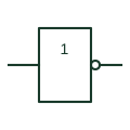
Single-input IEC box marked 1 with a negation at the output, inverting the logic state.
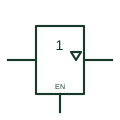
IEC buffer whose output carries the three-state triangle and is controlled by an EN input.
Elora Grid helps electrical teams work with drawings, specifications and equipment information. Explore the drafting workflow or join the early-access waitlist.