SR-LATCH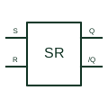
Set-reset latch
Retains a digital state that is changed by the defined set or reset input conditions.
Schematic
Two NAND gates with outputs fed back to each other, forming an SR latch with active-low set and reset.
In plain English
Drawing the latch as two cross-coupled NAND gates shows its construction explicitly. A low on the set input forces Q high; a low on the reset input forces the complement high. With both inputs high the latch holds. Both inputs low drives both outputs high, which is normally treated as invalid.
This drawing form is common in teaching material, switch debounce circuits and older schematics where the latch is built from a quad NAND package. It lets a reviewer see the feedback paths and the pins used.
Because the latch is built from gates, the drawing shows nothing about which state it adopts at power-up. If a defined state is needed, a reset pulse or a pull network must be shown.
Two NAND gates with outputs fed back to each other, forming an SR latch with active-low set and reset. The cross-coupled NOR latch has active-high inputs.
Read the source: SN74HC00 — NAND gate logic · SN74LS279A — set-reset latches
Distinctive-shape form as used in IEEE/ANSI-style schematics and manufacturer data books. Independent educational drawing; exact standard geometry and compliance are not asserted. The counterpart is the matching functional concept; no equivalence of every detailed standard graphic is asserted.
Shown as an independently authored educational illustration. Use the cited publication and drawing legend to verify the required drafting form.
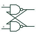
Drawing the latch as two cross-coupled NAND gates shows its construction explicitly. A low on the set input forces Q high; a low on the reset input forces the complement high. With both inputs high the latch holds. Both inputs low drives both outputs high, which is normally treated as invalid.
This drawing form is common in teaching material, switch debounce circuits and older schematics where the latch is built from a quad NAND package. It lets a reviewer see the feedback paths and the pins used.
Because the latch is built from gates, the drawing shows nothing about which state it adopts at power-up. If a defined state is needed, a reset pulse or a pull network must be shown.
The cross-coupled NOR latch has active-high inputs.
These public references support the explanation and provide further detail. Their graphics and downloadable files remain with their publishers.
NAND gate documentation for the building block.
SR latch device documentation.
This illustration was authored independently by Elora Grid to explain the concept. It is not reproduced from a customer drawing, an official standard graphic or a manufacturer CAD file. Its correspondence to an exact IEC or IEEE symbol identifier has not been certified.
SVG and DXF downloads contain this original artwork. DXF uses unscaled drawing units; a GA envelope supplies no product dimensions, clearances or fabrication information. Original artwork is available under CC BY 4.0. Third-party references retain their own terms.
Retains a digital state that is changed by the defined set or reset input conditions.
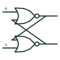
Two NOR gates cross-coupled to form an SR latch with active-high set and reset inputs.
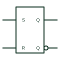
Rectangular IEC bistable with S and R inputs that set or reset the stored state immediately.
Elora Grid helps electrical teams work with drawings, specifications and equipment information. Explore the drafting workflow or join the early-access waitlist.