LEVEL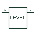
Logic voltage-level translator
Transfers digital information between the documented logic-voltage domains.
Schematic
In plain English
An I2C bus buffer separates or supports selected parts of an I2C connection.
A design can use a suitable buffer to manage loading between bus segments.
Show the bus segment on each side of the buffer and identify the clock and data paths. Buffers can manage electrical loading, but their permitted direction behaviour and connections vary. They should not be drawn as ordinary logic buffers without checking how they handle the selected I2C bus.
Not merely because it separates bus segments electrically for loading purposes. A rated isolation barrier is a different function and must be explicitly identified in the selected device.
Read the source: I2C, I3C and SPI interface functions
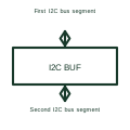
Buffer behaviour, direction handling and supported bus conditions depend on the selected device.
These public references support the explanation and provide further detail. Their graphics and downloadable files remain with their publishers.
I2C, I3C and SPI interface functions: public technical context for the named function. Product and compliance details remain with the publisher.
This illustration was authored independently by Elora Grid to explain the concept. It is not reproduced from a customer drawing, an official standard graphic or a manufacturer CAD file. Its correspondence to an exact IEC or IEEE symbol identifier has not been certified.
SVG and DXF downloads contain this original artwork. DXF uses unscaled drawing units; a GA envelope supplies no product dimensions, clearances or fabrication information. Original artwork is available under CC BY 4.0. Third-party references retain their own terms.
Transfers digital information between the documented logic-voltage domains.
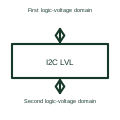
An I2C level translator adapts the specified logic-voltage levels between compatible bus sections.
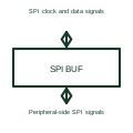
An SPI buffer supports the selected digital signal paths between an SPI controller and its peripheral interface.
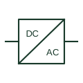
An identified interface converting electrical power between documented circuit forms.
Elora Grid helps electrical teams work with drawings, specifications and equipment information. Explore the drafting workflow or join the early-access waitlist.