SIPO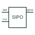
Serial-in parallel-out register
Shifts serial input data through storage stages to parallel outputs at the documented clock events.
Schematic
IEC register marked SRGm with m stages; the clock carries the shift arrow and moves data one place each cycle.
In plain English
SRGm identifies a shift register of m bits. The clock input is labelled with C1 and a shift arrow, showing that each active edge moves data one place. The serial input is labelled 1D, and the parallel outputs are listed down the right side, typically in a column of per-bit elements under a common-control block.
On drawings, shift registers expand outputs for indicators or relay drivers, or capture serial data from a sensor. The reader should identify the shift direction, the serial input, and any output latch or enable, as these decide how and when outputs update.
The symbol does not show the data rate or the serial protocol. Those come from the controller documentation driving the register.
IEC register marked SRGm with m stages; the clock carries the shift arrow and moves data one place each cycle. A latched shift register adds a storage register and its own clock between the shift stages and the outputs.
Read the source: Overview of IEEE Standard 91-1984: explanation of logic symbols (SDYZ001A) · SN74HC164 — serial-in parallel-out shift storage
Qualifying-symbol and dependency conventions as explained in TI's public overview of IEEE Std 91-1984, which incorporates IEC 617-12 work. Independent educational drawing; not certified IEC geometry or an IEC database identifier. The counterpart is the matching functional concept; no equivalence of every detailed standard graphic is asserted.
Shown as an independently authored educational illustration. Use the cited publication and drawing legend to verify the required drafting form.
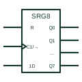
SRGm identifies a shift register of m bits. The clock input is labelled with C1 and a shift arrow, showing that each active edge moves data one place. The serial input is labelled 1D, and the parallel outputs are listed down the right side, typically in a column of per-bit elements under a common-control block.
On drawings, shift registers expand outputs for indicators or relay drivers, or capture serial data from a sensor. The reader should identify the shift direction, the serial input, and any output latch or enable, as these decide how and when outputs update.
The symbol does not show the data rate or the serial protocol. Those come from the controller documentation driving the register.
A latched shift register adds a storage register and its own clock between the shift stages and the outputs.
These public references support the explanation and provide further detail. Their graphics and downloadable files remain with their publishers.
Lists SRGm and shift right or left input labels.
Serial-in parallel-out shift register documentation.
This illustration was authored independently by Elora Grid to explain the concept. It is not reproduced from a customer drawing, an official standard graphic or a manufacturer CAD file. Its correspondence to an exact IEC or IEEE symbol identifier has not been certified.
SVG and DXF downloads contain this original artwork. DXF uses unscaled drawing units; a GA envelope supplies no product dimensions, clearances or fabrication information. Original artwork is available under CC BY 4.0. Third-party references retain their own terms.
Shifts serial input data through storage stages to parallel outputs at the documented clock events.
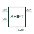
Combines a serial shift path with a separate output-storage stage.
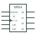
IEC shift register with mode inputs that select shift right, shift left, parallel load or hold.
Elora Grid helps electrical teams work with drawings, specifications and equipment information. Explore the drafting workflow or join the early-access waitlist.