AOI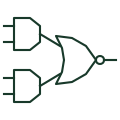
ANSI AND-OR-invert gate
Two D-shaped AND gates feeding a bubbled OR outline, drawn as the distinctive-shape AND-OR-invert function.
IEEE / ANSI
Two & elements embedded in a ≥1 element with negated output, drawn as one compound IEC AND-OR-invert symbol.
In plain English
The IEC system draws an AND-OR-invert as several & elements abutted against the left side of a ≥1 element, whose output is negated. Because the common line between the & and ≥1 parts is perpendicular to the signal flow, each & element is understood to feed one input of the OR.
AOI structures appear in older TTL-based control boards and in some gate-array documentation. On a drawing they compress several gates into one symbol, so the reader should expand the function mentally as the complement of a sum of products before checking a truth table.
The compound symbol does not show internal timing or whether unused AND inputs are tied. Unused inputs on the physical device must be handled as the datasheet requires.
Two & elements embedded in a ≥1 element with negated output, drawn as one compound IEC AND-OR-invert symbol. Separate AND gates wired to a NOR gate perform the same function but are drawn as distinct elements with visible interconnections.
Read the source: Overview of IEEE Standard 91-1984: explanation of logic symbols (SDYZ001A) · SN74LS51 AND-OR-invert gates
Qualifying-symbol and dependency conventions as explained in TI's public overview of IEEE Std 91-1984, which incorporates IEC 617-12 work. Independent educational drawing; not certified IEC geometry or an IEC database identifier.
Shown as an independently authored educational illustration. Use the cited publication and drawing legend to verify the required drafting form.
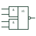
The IEC system draws an AND-OR-invert as several & elements abutted against the left side of a ≥1 element, whose output is negated. Because the common line between the & and ≥1 parts is perpendicular to the signal flow, each & element is understood to feed one input of the OR.
AOI structures appear in older TTL-based control boards and in some gate-array documentation. On a drawing they compress several gates into one symbol, so the reader should expand the function mentally as the complement of a sum of products before checking a truth table.
The compound symbol does not show internal timing or whether unused AND inputs are tied. Unused inputs on the physical device must be handled as the datasheet requires.
Separate AND gates wired to a NOR gate perform the same function but are drawn as distinct elements with visible interconnections.
These public references support the explanation and provide further detail. Their graphics and downloadable files remain with their publishers.
Explains abutted and embedded outlines and their implied connections.
Manufacturer AND-OR-invert gate documentation.
This illustration was authored independently by Elora Grid to explain the concept. It is not reproduced from a customer drawing, an official standard graphic or a manufacturer CAD file. Its correspondence to an exact IEC or IEEE symbol identifier has not been certified.
SVG and DXF downloads contain this original artwork. DXF uses unscaled drawing units; a GA envelope supplies no product dimensions, clearances or fabrication information. Original artwork is available under CC BY 4.0. Third-party references retain their own terms.
Two D-shaped AND gates feeding a bubbled OR outline, drawn as the distinctive-shape AND-OR-invert function.
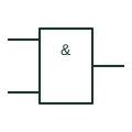
Rectangular IEC-style AND element marked with an ampersand; the output is active only when every input is active.
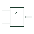
IEC ≥1 element with a negated output; the output is active only when none of the inputs are active.
Elora Grid helps electrical teams work with drawings, specifications and equipment information. Explore the drafting workflow or join the early-access waitlist.