BUS-TR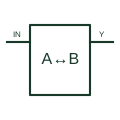
Logic bus transceiver
Drives data between two digital buses according to the selected direction and enable conditions.
Schematic
In plain English
An LVDS receiver converts a compatible differential input into its specified logic output.
The receiving end of a link can recover the logic state from the differential pair.
Identify the differential input pair and the receiver’s logic output. The pair’s valid input conditions and the output’s logic levels are separate specifications. Keep the sender and receiver labels visible so the drawing describes a complete direction of information flow.
Not necessarily. The receiver converts the selected differential input into its specified logic output. Both sides’ electrical requirements must be checked for the actual device.
Read the source: Low-voltage differential signalling
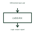
A receiver's accepted input conditions and output logic levels are separate specifications.
These public references support the explanation and provide further detail. Their graphics and downloadable files remain with their publishers.
Low-voltage differential signalling: public technical context for the named function. Product and compliance details remain with the publisher.
This illustration was authored independently by Elora Grid to explain the concept. It is not reproduced from a customer drawing, an official standard graphic or a manufacturer CAD file. Its correspondence to an exact IEC or IEEE symbol identifier has not been certified.
SVG and DXF downloads contain this original artwork. DXF uses unscaled drawing units; a GA envelope supplies no product dimensions, clearances or fabrication information. Original artwork is available under CC BY 4.0. Third-party references retain their own terms.
Drives data between two digital buses according to the selected direction and enable conditions.
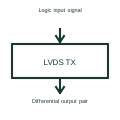
An LVDS driver converts a logic signal into the selected low-voltage differential output.
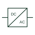
An identified interface converting electrical power between documented circuit forms.

An identified electrical connection point linking schematic and wiring information.
Elora Grid helps electrical teams work with drawings, specifications and equipment information. Explore the drafting workflow or join the early-access waitlist.