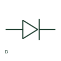
N-MOS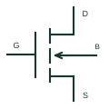
N-channel enhancement MOSFET
An insulated-gate transistor whose N-channel conduction is enabled by the documented gate-to-source drive.
Schematic
An N-channel insulated-gate device that conducts at zero gate-to-source voltage according to its device characteristics.
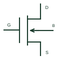
An N-channel insulated-gate device that conducts at zero gate-to-source voltage according to its device characteristics.
On a schematic, identify the gate bias needed to reduce conduction and the source reference and trace the bias, current-limiting or switching circuit. Keep the component tag and signal/reference names consistent across the control drawing, terminal schedule and device documentation.
Depletion-mode conduction at zero gate bias differs from enhancement mode and changes the circuit's default state.
Terminal letters describe electrical roles, not package pin numbers. Check the selected public datasheet for the actual pin assignment, polarity and any internally connected terminals before completing the drawing.
Depletion-mode conduction at zero gate bias differs from enhancement mode and changes the circuit's default state.
These public references support the explanation and provide further detail. Their graphics and downloadable files remain with their publishers.
Public primary manufacturer documentation establishes the component function or circuit/topology relationship. Preview geometry and drafting explanations are independently authored.
This illustration was authored independently by Elora Grid to explain the concept. It is not reproduced from a customer drawing, an official standard graphic or a manufacturer CAD file. Its correspondence to an exact IEC or IEEE symbol identifier has not been certified.
SVG and DXF downloads contain this original artwork. DXF uses unscaled drawing units; a GA envelope supplies no product dimensions, clearances or fabrication information. Original artwork is available under CC BY 4.0. Third-party references retain their own terms.
Elora Grid helps electrical teams work with drawings, specifications and equipment information. Explore the drafting workflow or join the early-access waitlist.