NAND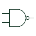
NAND gate
A logic gate that inverts the result of an AND operation.
Schematic
OR outline with bubbles on its inputs: the De Morgan form of a NAND used when inputs are active low.
In plain English
By De Morgan's theorem, a NAND gate is equivalent to an OR gate whose inputs are inverted. Data books and well-drawn schematics use the OR outline with input bubbles when the inputs are active-low signals, so that the drawing reads as any of these low signals produces a high output.
This form is useful where active-low requests or fault lines are combined. Matching bubbles to active-low nets lets a reader follow the logic without mentally inverting each signal, which is the main reason for choosing this representation.
The symbol represents the same physical part as the conventional NAND outline. It does not mean an OR device and inverters are fitted, and the bill of materials will still list a NAND package.
OR outline with bubbles on its inputs: the De Morgan form of a NAND used when inputs are active low. An OR outline with a bubble at the output is a NOR, not this NAND equivalent.
Read the source: SN74HC00 — NAND gate logic · Overview of IEEE Standard 91-1984: explanation of logic symbols (SDYZ001A)
Distinctive-shape form as used in IEEE/ANSI-style schematics and manufacturer data books. Independent educational drawing; exact standard geometry and compliance are not asserted. The counterpart is the matching functional concept; no equivalence of every detailed standard graphic is asserted.
Shown as an independently authored educational illustration. Use the cited publication and drawing legend to verify the required drafting form.
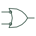
By De Morgan's theorem, a NAND gate is equivalent to an OR gate whose inputs are inverted. Data books and well-drawn schematics use the OR outline with input bubbles when the inputs are active-low signals, so that the drawing reads as any of these low signals produces a high output.
This form is useful where active-low requests or fault lines are combined. Matching bubbles to active-low nets lets a reader follow the logic without mentally inverting each signal, which is the main reason for choosing this representation.
The symbol represents the same physical part as the conventional NAND outline. It does not mean an OR device and inverters are fitted, and the bill of materials will still list a NAND package.
An OR outline with a bubble at the output is a NOR, not this NAND equivalent.
These public references support the explanation and provide further detail. Their graphics and downloadable files remain with their publishers.
Manufacturer NAND gate documentation for the implementing device.
Explains negation and active-low indication at inputs.
This illustration was authored independently by Elora Grid to explain the concept. It is not reproduced from a customer drawing, an official standard graphic or a manufacturer CAD file. Its correspondence to an exact IEC or IEEE symbol identifier has not been certified.
SVG and DXF downloads contain this original artwork. DXF uses unscaled drawing units; a GA envelope supplies no product dimensions, clearances or fabrication information. Original artwork is available under CC BY 4.0. Third-party references retain their own terms.
A logic gate that inverts the result of an AND operation.
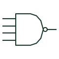
Four-input D-shaped NAND gate with an output bubble; its output goes low only when all four inputs are high.
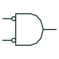
AND outline with bubbled inputs, the De Morgan form of a NOR that reads as all inputs low gives a high output.
Elora Grid helps electrical teams work with drawings, specifications and equipment information. Explore the drafting workflow or join the early-access waitlist.